The latest research of avalanche photodetector
Infrared detection technology is widely used in military reconnaissance, environmental monitoring, medical diagnosis and other fields. Traditional infrared detectors have some limitations in performance, such as detection sensitivity, response speed and so on. InAs/InAsSb Class II superlattice (T2SL) materials have excellent photoelectric properties and tunability, making them ideal for long-wave infrared (LWIR) detectors. The problem of weak response in long wave infrared detection has been a concern for a long time, which greatly limits the reliability of electronic device applications. Although avalanche photodetector (APD photodetector) has excellent response performance, it suffers from high dark current during multiplication.
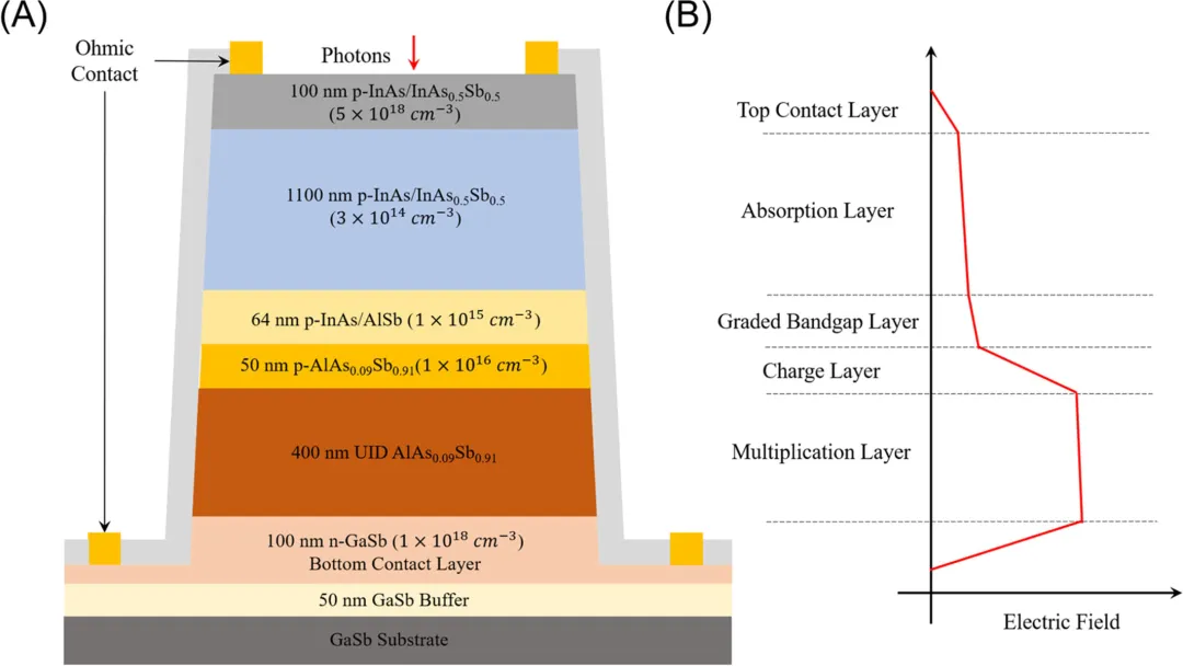
To solve these problems, a team from the University of Electronic Science and Technology of China has successfully designed a high-performance Class II superlattice (T2SL) long-wave infrared avalanche photodiode (APD). The researchers used the lower auger recombination rate of the InAs/InAsSb T2SL absorber layer to reduce the dark current. At the same time, AlAsSb with low k value is used as the multiplier layer to suppress device noise while maintaining sufficient gain. This design provides a promising solution for promoting the development of long wave infrared detection technology. The detector adopts a stepped tiered design, and by adjusting the composition ratio of InAs and InAsSb, the smooth transition of the band structure is achieved, and the performance of the detector is improved. In terms of material selection and preparation process, this study describes in detail the growth method and process parameters of InAs/InAsSb T2SL material used to prepare the detector. Determining the composition and thickness of InAs/InAsSb T2SL is critical and parameter adjustment is required to achieve stress balance. In the context of long-wave infrared detection, to achieve the same cut-off wavelength as InAs/GaSb T2SL, a thicker InAs/InAsSb T2SL single period is required. However, thicker monocycle results in a decrease in the absorption coefficient in the direction of growth and an increase in the effective mass of holes in T2SL. It is found that adding Sb component can achieve longer cutoff wavelength without significantly increasing single period thickness. However, excessive Sb composition may lead to segregation of Sb elements.
Therefore, InAs/InAs0.5Sb0.5 T2SL with Sb group 0.5 was selected as the active layer of APD photodetector. InAs/InAsSb T2SL mainly grows on GaSb substrates, so the role of GaSb in strain management needs to be considered. Essentially, achieving strain equilibrium involves comparing the average lattice constant of a superlattice for one period to the lattice constant of the substrate. Generally, the tensile strain in the InAs is compensated by the compressive strain introduced by the InAsSb, resulting in a thicker InAs layer than the InAsSb layer. This study measured the photoelectric response characteristics of the avalanche photodetector, including spectral response, dark current, noise, etc., and verified the effectiveness of the stepped gradient layer design. The avalanche multiplication effect of the avalanche photodetector is analyzed, and the relationship between the multiplication factor and the incident light power, temperature and other parameters is discussed.

FIG. (A) Schematic diagram of InAs/InAsSb long-wave infrared APD photodetector; (B) Schematic diagram of electric fields at each layer of APD photodetector.
Post time: Jan-06-2025


