For silicon-based optoelectronics, silicon photodetectors
Photodetectors convert light signals into electrical signals, and as data transfer rates continue to improve, high-speed photodetectors integrated with silicon-based optoelectronics platforms have become key to next-generation data centers and telecommunications networks. This article will provide an overview of advanced high-speed photodetectors, with emphasis on silicon based germanium (Ge or Si photodetector) silicon photodetectors for integrated optoelectronics technology.
Germanium is an attractive material for near infrared light detection on silicon platforms because it is compatible with CMOS processes and has extremely strong absorption at telecommunication wavelengths. The most common Ge/Si photodetector structure is the p-i-n diode, in which the intrinsic germanium is sandwiched between the P-type and N-type regions.

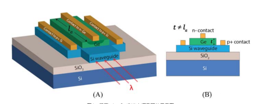
Device structure Figure 1 shows a typical vertical p-i-n Ge or Si photodetector structure:
The main features include: germanium absorbing layer grown on silicon substrate; Used to collect p and n contacts of charge carriers; Waveguide coupling for efficient light absorption.
Epitaxial growth: Growing high quality germanium on silicon is challenging due to the 4.2% lattice mismatch between the two materials. A two-step growth process is usually used: low temperature (300-400°C) buffer layer growth and high temperature (above 600°C) deposition of germanium. This method helps to control threading dislocations caused by lattice mismatches. Post-growth annealing at 800-900°C further reduces the threading dislocation density to about 10^7 cm^-2. Performance characteristics: The most advanced Ge/Si PIN photodetector can achieve: responsiveness, > 0.8A /W at 1550 nm; Bandwidth,>60 GHz; Dark current, <1 μA at -1 V bias.
Integration with silicon-based optoelectronics platforms
The integration of high-speed photodetectors with silicon-based optoelectronics platforms enables advanced optical transceivers and interconnects. The two main integration methods are as follows: Front-end integration (FEOL), where the photodetector and transistor are simultaneously manufactured on a silicon substrate allowing for high-temperature processing, but taking up chip area. Back-end integration (BEOL). Photodetectors are manufactured on top of the metal to avoid interference with CMOS, but are limited to lower processing temperatures.

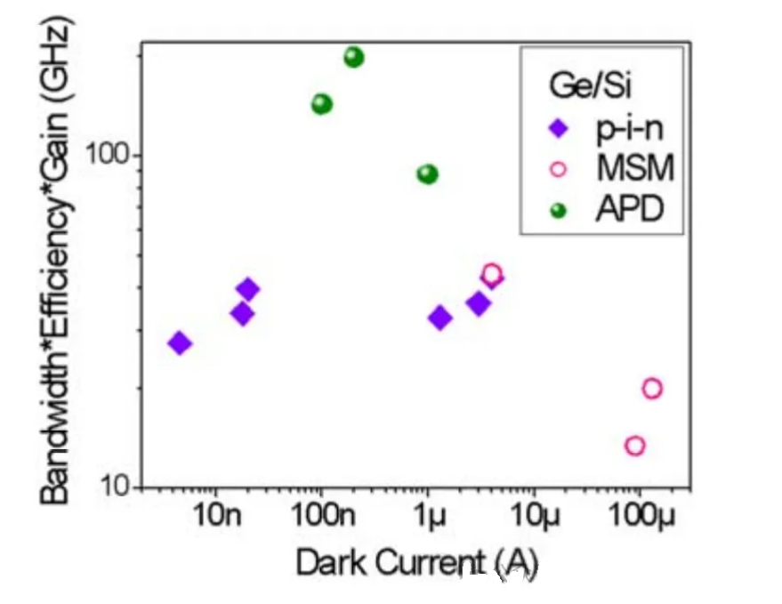
Figure 2: Responsiveness and bandwidth of a high-speed Ge/Si photodetector
Data center application
High-speed photodetectors are a key component in the next generation of data center interconnection. Main applications include: optical transceivers :100G, 400G and higher rates, using PAM-4 modulation; A high bandwidth photodetector (>50 GHz) is required.
Silicon-based optoelectronic integrated circuit: monolithic integration of detector with modulator and other components; A compact, high-performance optical engine.
Distributed architecture: optical interconnection between distributed computing, storage, and storage; Driving the demand for energy-efficient, high-bandwidth photodetectors.
Future outlook
The future of integrated optoelectronic high-speed photodetectors will show the following trends:
Higher data rates: Driving the development of 800G and 1.6T transceivers; Photodetectors with bandwidths greater than 100 GHz are required.
Improved integration: Single chip integration of III-V material and silicon; Advanced 3D integration technology.
New materials: Exploring two-dimensional materials (such as graphene) for ultrafast light detection; A new Group IV alloy for extended wavelength coverage.
Emerging applications: LiDAR and other sensing applications are driving the development of APD; Microwave photon applications requiring high linearity photodetectors.
High-speed photodetectors, especially Ge or Si photodetectors, have become a key driver of silicon-based optoelectronics and next-generation optical communications. Continued advances in materials, device design, and integration technologies are important to meet the growing bandwidth demands of future data centers and telecommunications networks. As the field continues to evolve, we can expect to see photodetectors with higher bandwidth, lower noise, and seamless integration with electronic and photonic circuits.
Post time: Jan-20-2025


