Photonic integrated circuit (PIC) material system
Silicon photonics is a discipline that uses planar structures based on silicon materials to direct light to achieve a variety of functions. We focus here on the application of silicon photonics in creating transmitters and receivers for fiber optic communications. As the need to add more transmission at a given bandwidth, a given footprint, and a given cost increases, silicon photonics becomes more economically sound. For the optical part, photonic integration technology must be used, and most coherent transceivers today are built using separate LiNbO3/ planar light-wave circuit (PLC) modulators and InP/PLC receivers.

Figure 1: Shows commonly used photonic integrated circuit (PIC) material systems.
Figure 1 shows the most popular PIC material systems. From left to right are silicon-based silica PIC (also known as PLC), silicon-based insulator PIC (silicon photonics), lithium niobate (LiNbO3), and III-V group PIC, such as InP and GaAs. This paper focuses on silicon-based photonics. In silicon photonics, the light signal mainly travels in silicon, which has an indirect band gap of 1.12 electron volts (with a wavelength of 1.1 microns). Silicon is grown in the form of pure crystals in furnaces and then cut into wafers, which today are typically 300 mm in diameter. The wafer surface is oxidized to form a silica layer. One of the wafers is bombarded with hydrogen atoms to a certain depth. The two wafers are then fused in a vacuum and their oxide layers bond to each other. The assembly breaks along the hydrogen ion implantation line. The silicon layer at the crack is then polished, eventually leaving a thin layer of crystalline Si on top of the intact silicon “handle” wafer on top of the silica layer. Waveguides are formed from this thin crystalline layer. While these silicon-based insulator (SOI) wafers make low-loss silicon photonics waveguides possible, they are actually more commonly used in low-power CMOS circuits because of the low leakage current they provide.
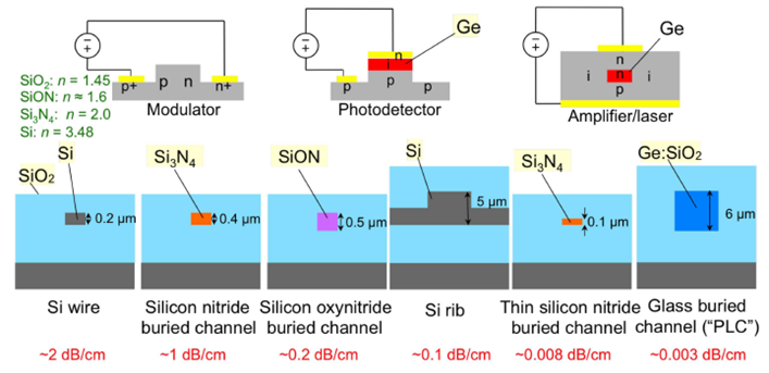
There are many possible forms of silicon-based optical waveguides, as shown in Figure 2. They range from microscale germanium-doped silica waveguides to nanoscale Silicon Wire waveguides. By blending germanium, it is possible to make photodetectors and electrical absorption modulators, and possibly even optical amplifiers. By doping silicon, an optical modulator can be made. The bottom from left to right are: silicon wire waveguide, silicon nitride waveguide, silicon oxynitride waveguide, thick silicon ridge waveguide, thin silicon nitride waveguide and doped silicon waveguide. At the top, from left to right, are depletion modulators, germanium photodetectors, and germanium optical amplifiers.

Figure 2: Cross-section of a silicon-based optical waveguide series, showing typical propagation losses and refractive indices.
Post time: Jul-15-2024


