New technology of thin silicon photodetector
Photon capture structures are used to enhance light absorption in thin silicon photodetectors
Photonic systems are rapidly gaining traction in many emerging applications, including optical communications, liDAR sensing, and medical imaging. However, the widespread adoption of photonics in future engineering solutions depends on the cost of manufacturing photodetectors, which in turn depends largely on the type of semiconductor used for that purpose.
Traditionally, silicon (Si) has been the most ubiquitous semiconductor in the electronics industry, so much so that most industries have matured around this material. Unfortunately, Si has a relatively weak light absorption coefficient in the near infrared (NIR) spectrum compared to other semiconductors such as gallium arsenide (GaAs). Because of this, GaAs and related alloys are thriving in photonic applications but are not compatible with the traditional complementary metal-oxide semiconductor (CMOS) processes used in the production of most electronics. This led to a sharp increase in their manufacturing costs.
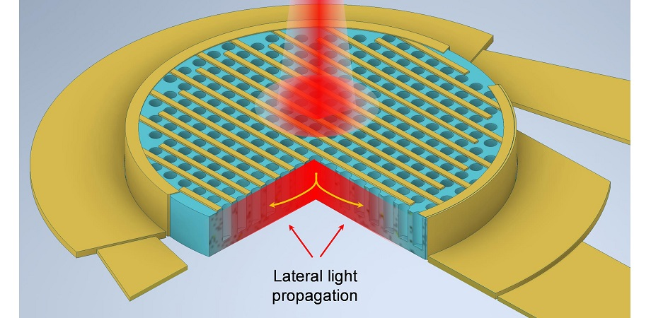
Researchers have devised a way to greatly enhance near-infrared absorption in silicon, which could lead to cost reductions in high-performance photonic devices, and a UC Davis research team is pioneering a new strategy to greatly improve light absorption in silicon thin films. In their latest paper at Advanced Photonics Nexus, they demonstrate for the first time an experimental demonstration of a silicon-based photodetector with light-capturing micro – and nano-surface structures, achieving unprecedented performance improvements comparable to GaAs and other III-V group semiconductors. The photodetector consists of a micron-thick cylindrical silicon plate placed on an insulating substrate, with metal “fingers” extending in a finger-fork fashion from the contact metal at the top of the plate. Importantly, the lumpy silicon is filled with circular holes arranged in a periodic pattern that act as photon capture sites. The overall structure of the device causes the normally incident light to bend by nearly 90° when it hits the surface, allowing it to propagate laterally along the Si plane. These lateral propagation modes increase the length of light’s travel and effectively slow it down, leading to more light-matter interactions and thus increased absorption.
The researchers also conducted optical simulations and theoretical analyses to better understand the effects of photon capture structures, and conducted several experiments comparing photodetectors with and without them. They found that photon capture led to a significant improvement in broadband absorption efficiency in the NIR spectrum, staying above 68% with a peak of 86%. It is worth noting that in the near infrared band, the absorption coefficient of the photon capture photodetector is several times higher than that of ordinary silicon, exceeding gallium arsenide. In addition, although the proposed design is for 1μm thick silicon plates, simulations of 30 nm and 100 nm silicon films compatible with CMOS electronics show similar enhanced performance.
Overall, the results of this study demonstrate a promising strategy for improving the performance of silicon-based photodetectors in emerging photonics applications. High absorption can be achieved even in ultra-thin silicon layers, and the circuit’s parasitic capacitance can be kept low, which is critical in high-speed systems. In addition, the proposed method is compatible with modern CMOS manufacturing processes and therefore has the potential to revolutionize the way optoelectronics are integrated into traditional circuits. This, in turn, could pave the way for substantial leaps in affordable ultrafast computer networks and imaging technology.

Post time: Nov-12-2024


