High speed photodetectors are introduced by InGaAs photodetectors
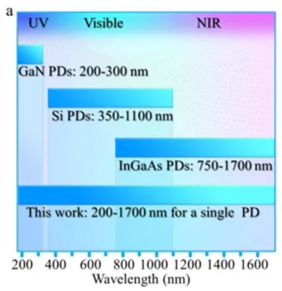
High-speed photodetectors in the field of optical communication mainly include III-V InGaAs photodetectors and IV full Si and Ge/Si photodetectors. The former is a traditional near infrared detector, which has been dominant for a long time, while the latter relies on silicon optical technology to become a rising star, and is a hot spot in the field of international optoelectronics research in recent years. In addition, new detectors based on perovskite, organic and two-dimensional materials are developing rapidly due to the advantages of easy processing, good flexibility and tunable properties. There are significant differences between these new detectors and traditional inorganic photodetectors in material properties and manufacturing processes. Perovskite detectors have excellent light absorption characteristics and efficient charge transport capacity, organic materials detectors are widely used for their low cost and flexible electrons, and two-dimensional materials detectors have attracted much attention due to their unique physical properties and high carrier mobility. However, compared with InGaAs and Si/Ge detectors, the new detectors still need to be improved in terms of long-term stability, manufacturing maturity and integration.
InGaAs is one of the ideal materials for realizing high speed and high response photodetectors. First of all, InGaAs is a direct bandgap semiconductor material, and its bandgap width can be regulated by the ratio between In and Ga to achieve the detection of optical signals of different wavelengths. Among them, In0.53Ga0.47As is perfectly matched with the substrate lattice of InP, and has a large light absorption coefficient in the optical communication band, which is the most widely used in the preparation of photodetectors, and the dark current and responsiveness performance are also the best. Secondly, InGaAs and InP materials both have high electron drift velocity, and their saturated electron drift velocity is about 1×107 cm/s. At the same time, InGaAs and InP materials have electron velocity overshoot effect under specific electric field. The overshoot velocity can be divided into 4× 107cm/s and 6×107cm/s, which is conducive to realizing a larger carrier time-limited bandwidth. At present, InGaAs photodetector is the most mainstream photodetector for optical communication, and the surface incidence coupling method is mostly used in the market, and the 25 Gbaud/s and 56 Gbaud/s surface incidence detector products have been realized. Smaller size, back incidence and large bandwidth surface incidence detectors have also been developed, which are mainly suitable for high speed and high saturation applications. However, the surface incident probe is limited by its coupling mode and is difficult to integrate with other optoelectronic devices. Therefore, with the improvement of optoelectronic integration requirements, waveguide coupled InGaAs photodetectors with excellent performance and suitable for integration have gradually become the focus of research, among which the commercial 70 GHz and 110 GHz InGaAs photoprobe modules are almost all using waveguide coupled structures. According to the different substrate materials, the waveguide coupling InGaAs photoelectric probe can be divided into two categories: InP and Si. The epitaxial material on InP substrate has high quality and is more suitable for the preparation of high-performance devices. However, various mismatches between III-V materials, InGaAs materials and Si substrates grown or bonded on Si substrates lead to relatively poor material or interface quality, and the performance of the device still has a large room for improvement.
Post time: Dec-31-2024


