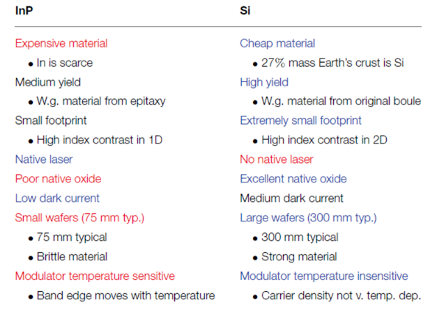
Comparison of photonic integrated circuit material systems
Figure 1 shows a comparison of two material systems, indium Phosphorus (InP) and silicon (Si). The rarity of indium makes InP a more expensive material than Si. Because silicon-based circuits involve less epitaxial growth, the yield of silicon-based circuits is usually higher than that of InP circuits. In silicon-based circuits, germanium (Ge), which is usually only used in Photodetector (light detectors), requires epitaxial growth, while in InP systems, even passive waveguides must be prepared by epitaxial growth. Epitaxial growth tends to have a higher defect density than single crystal growth, such as from a crystal ingot. InP waveguides have high refractive index contrast only in transverse, while silicon-based waveguides have high refractive index contrast in both transverse and longitudinal, which allows silicon-based devices to achieve smaller bending radii and other more compact structures. InGaAsP has a direct band gap, while Si and Ge do not. As a result, InP material systems are superior in terms of laser efficiency. The intrinsic oxides of InP systems are not as stable and robust as the intrinsic oxides of Si, silicon dioxide (SiO2). Silicon is a stronger material than InP, allowing the use of larger wafer sizes, i.e. from 300 mm (soon to be upgraded to 450 mm) compared to 75 mm in InP. InP modulators usually depend on the quantum-confined Stark effect, which is temperature-sensitive due to band edge movement caused by temperature. In contrast, the temperature dependence of silicon-based modulators is very small.

Silicon photonics technology is generally considered only suitable for low-cost, short-range, high-volume products (more than 1 million pieces per year). This is because it is widely accepted that a large amount of wafer capacity is required to spread mask and development costs, and that silicon photonics technology has significant performance disadvantages in city-to-city regional and long-haul product applications. In reality, however, the opposite is true. In low-cost, short-range, high-yield applications, vertical cavity surface-emitting laser (VCSEL) and direct-modulated laser (DML laser) : directly modulated laser poses a huge competitive pressure, and the weakness of silicon-based photonic technology that cannot easily integrate lasers has become a significant disadvantage. In contrast, in metro, long-distance applications, due to the preference for integrating silicon photonics technology and digital signal processing (DSP) together (which is often in high temperature environments), it is more advantageous to separate the laser. In addition, coherent detection technology can make up for the shortcomings of silicon photonics technology to a large extent, such as the problem that the dark current is much smaller than the local oscillator photocurrent. At the same time, it is also wrong to think that a large amount of wafer capacity is needed to cover mask and development costs, because silicon photonics technology uses node sizes that are much larger than the most advanced complementary metal oxide semiconductors (CMOS), so the required masks and production runs are relatively cheap.
Post time: Aug-02-2024


