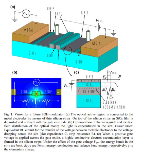
One of the most important properties of an optical modulator is its modulation speed or bandwidth, which should be at least as fast as the available electronics. Transistors having transit frequencies well above 100 GHz have already been demonstrated in 90 nm silicon technology, and the speed will further increase as the minimum feature size is reduced [1]. However, the bandwidth of present-day silicon-based modulators is limited. Silicon does not possess a χ(2)-nonlinearity due to its centro-symmetric crystalline structure. The use of strained silicon has led to interesting results already [2], but the nonlinearities do not yet allow for practical devices. State-of-the art silicon photonic modulators therefore still rely on free-carrier dispersion in pn or pin junctions [3–5]. Forward biased junctions have been shown to exhibit a voltage-length product as low as VπL = 0.36 V mm, but the modulation speed is limited by the dynamics of minority carriers. Still, data rates of 10 Gbit/s have been generated with the help of a pre-emphasis of the electrical signal [4]. Using reverse biased junctions instead, the bandwidth has been increased to about 30 GHz [5,6], but the voltagelength product rose to VπL = 40 V mm. Unfortunately, such plasma effect phase modulators produce undesired intensity modulation as well [7], and they respond nonlinearly to the applied voltage. Advanced modulation formats like QAM require, however, a linear response and pure phase modulation, making the exploitation of the electro-optic effect (Pockels effect [8]) particularly desirable.
2. SOH approach
Recently, the silicon-organic hybrid (SOH) approach has been suggested [9–12]. An example of an SOH modulator is shown in Fig. 1(a). It consists of a slot waveguide guiding the optical field, and two silicon strips which electrically connect the optical waveguide to the metallic electrodes. The electrodes are located outside the optical modal field to avoid optical losses [13], Fig. 1(b). The device is coated with an electro-optic organic material which uniformly fills the slot. The modulating voltage is carried by the metallic electrical waveguide and drops off across the slot thanks to the conductive silicon strips. The resulting electric field then changes the index of refraction in the slot through the ultra-fast electro-optic effect. Since the slot has a width in the order of 100 nm, a few volts are enough to generate very strong modulating fields which are in the order of magnitude of the dielectric strength of most materials. The structure has a high modulation efficiency since both the modulating and the optical fields are concentrated inside the slot, Fig. 1(b) [14]. Indeed, first implementations of SOH modulators with sub-volt operation [11] have been already shown, and sinusoidal modulation up to 40 GHz was demonstrated [15,16]. However, the challenge in building low-voltage high-speed SOH modulators is to create a highly conductive connecting strip. In an equivalent circuit the slot can be represented by a capacitor C and the conductive strips by resistors R, Fig. 1(b). The corresponding RC time constant determines the bandwidth of the device [10,14,17,18]. In order to decrease the resistance R, it has been suggested to dope the silicon strips [10,14]. While doping increases the conductivity of the silicon strips (and therefore increases optical losses), one pays an additional loss penalty because the electron mobility is impaired by impurity scattering [10,14,19]. Moreover, the most recent fabrication attempts showed unexpectedly low conductivity.

Beijing Rofea Optoelectronics Co., Ltd. located in China’s “Silicon Valley” – Beijing Zhongguancun, is a high-tech enterprise dedicated to serving domestic and foreign research institutions, research institutes, universities and enterprise scientific research personnel. Our company is mainly engaged in the independent research and development, design, manufacturing, sales of optoelectronic products, and provides innovative solutions and professional, personalized services for scientific researchers and industrial engineers. After years of independent innovation, it has formed a rich and perfect series of photoelectric products, which are widely used in municipal, military, transportation, electric power, finance, education, medical and other industries.
We are looking forward to cooperation with you!
Post time: Mar-29-2023


